

01 / LARGE AREA SCAN
Large-Area Fast Scanning
From wafers to full glass panels, see the complete surface quickly.
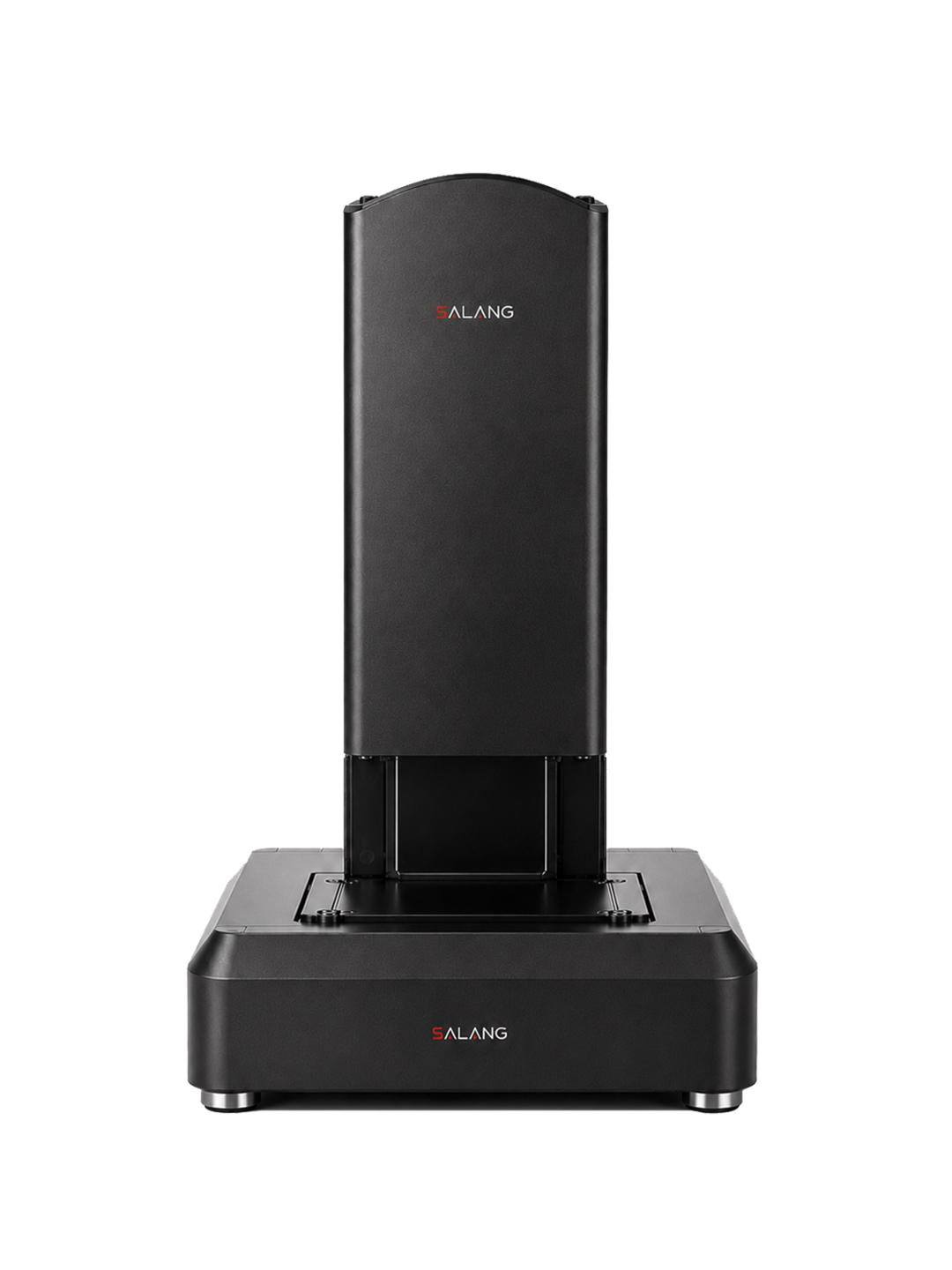
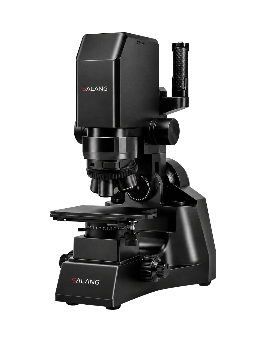
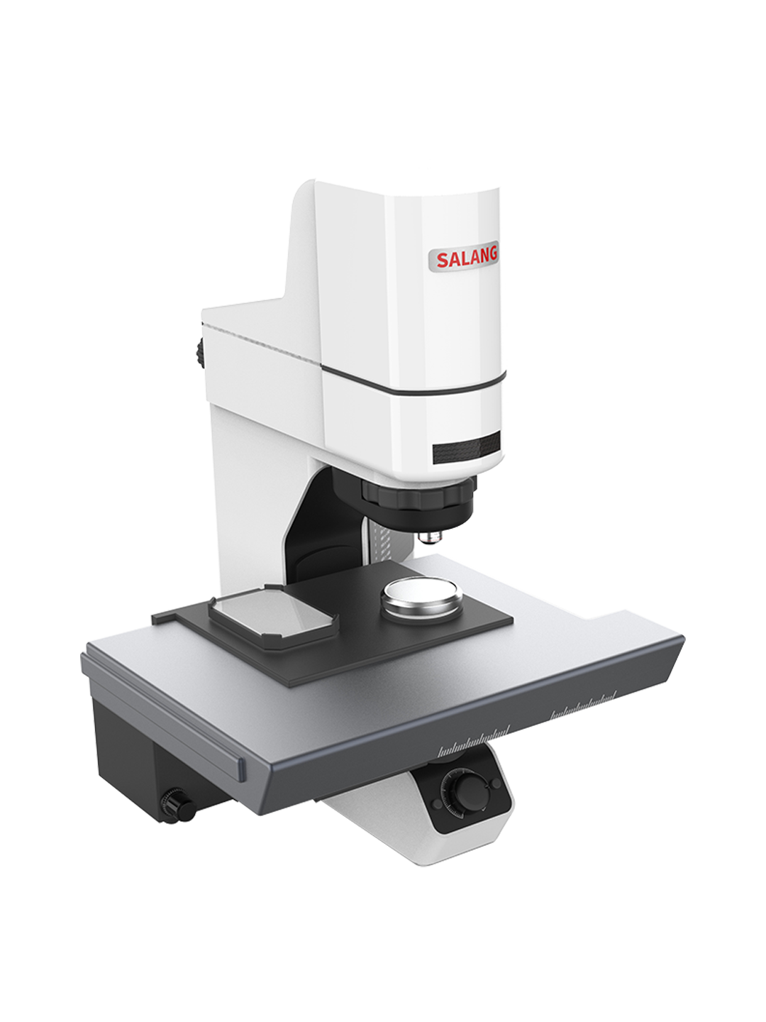
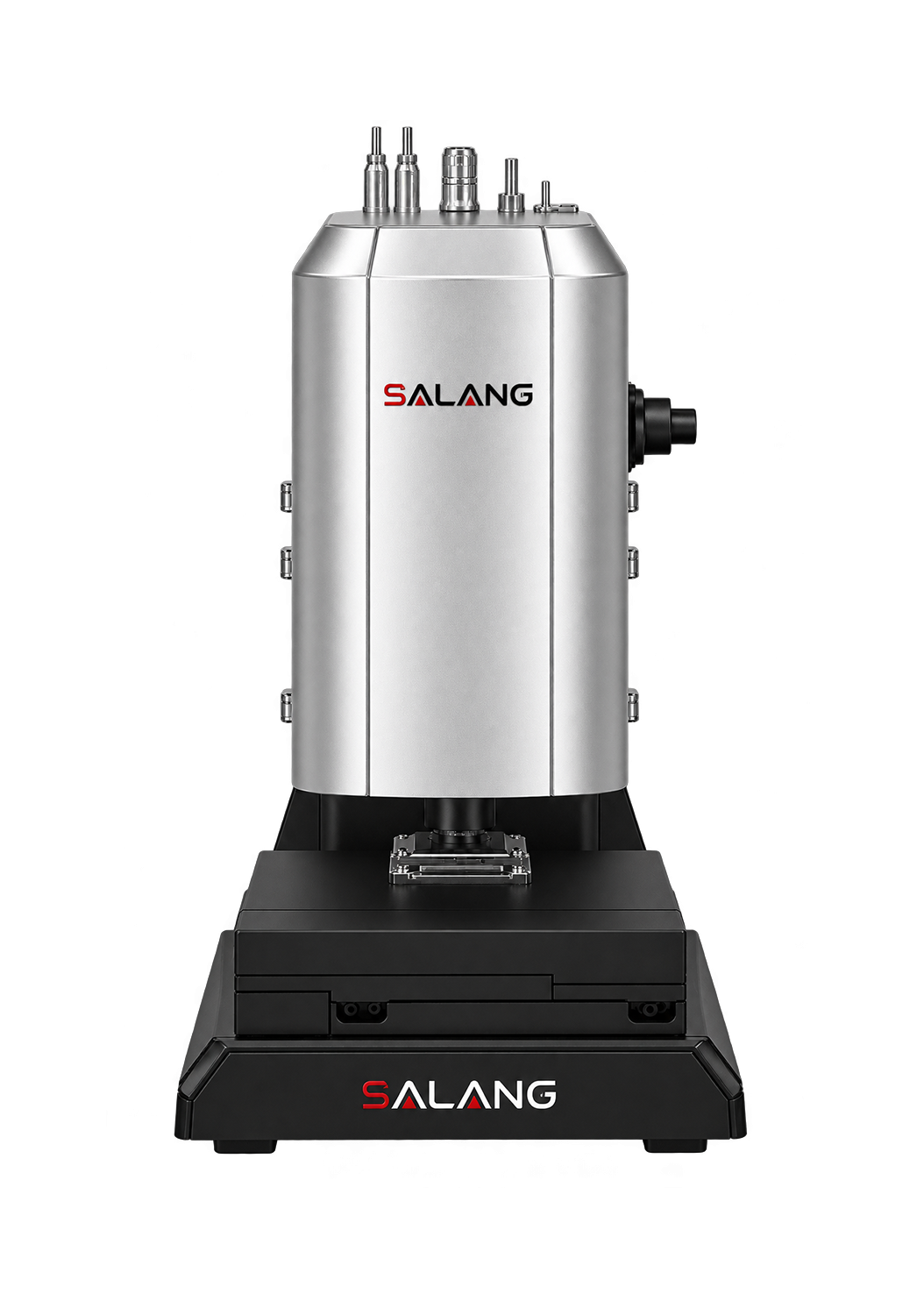
SA-1000 supports large-area fast scanning: 300 × 300 mm in about 150 s, 400 × 400 mm in about 260 s, and 500 × 500 mm in about 350 s. It is suitable for rapid mapping and surface-defect localization on wafers, glass, films, electrodes and other large flat samples.
View Product